Author Affiliations
Abstract
1 Key Laboratory of Nanodevices and Applications, Suzhou Institute of Nano-tech and Nano-Bionics, Chinese Academy of Sciences, Suzhou 215123, China
2 School of Physical Science and Technology, ShanghaiTech University, Shanghai 201210, China
3 Shanghai Advanced Research Institute, Chinese Academy of Sciences, Shanghai 201210, China
4 University of Chinese Academy of Sciences, Beijing 100049, China
A new kind of step-flow growth mode is proposed, which adopts sidewall as step source on patterned GaN substrate. The terrace width of steps originated from the sidewall was found to change with the growth temperature and ammonia flux. The growth mechanism is explained and simulated based on step motion model. This work helps better understand the behaviors of step advancement and puts forward a method of precisely modulating atomic steps.
step-flow growth GaN terrace width step motion Journal of Semiconductors
2024, 45(2): 022501
Author Affiliations
Abstract
1 School of Nano-Tech and Nano-Bionics, University of Science and Technology of China, Hefei 230026, China
2 Suzhou Institute of Nano-Tech and Nano-Bionics, Chinese Academy of Sciences, Suzhou 215123, China
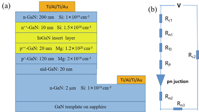
The InGaN films and GaN/InGaN/GaN tunnel junctions (TJs) were grown on GaN templates with plasma-assisted molecular beam epitaxy. As the In content increases, the quality of InGaN films grown on GaN templates decreases and the surface roughness of the samples increases. V-pits and trench defects were not found in the AFM images. p++-GaN/InGaN/n++-GaN TJs were investigated for various In content, InGaN thicknesses and doping concentration in the InGaN insert layer. The InGaN insert layer can promote good interband tunneling in GaN/InGaN/GaN TJ and significantly reduce operating voltage when doping is sufficiently high. The current density increases with increasing In content for the 3 nm InGaN insert layer, which is achieved by reducing the depletion zone width and the height of the potential barrier. At a forward current density of 500 A/cm2, the measured voltage was 4.31 V and the differential resistance was measured to be 3.75 × 10?3 Ω·cm2 for the device with a 3 nm p++-In0.35Ga0.65N insert layer. When the thickness of the In0.35Ga0.65N layer is closer to the “balanced” thickness, the TJ current density is higher. If the thickness is too high or too low, the width of the depletion zone will increase and the current density will decrease. The undoped InGaN layer has a better performance than n-type doping in the TJ. Polarization-engineered tunnel junctions can enhance the functionality and performance of electronic and optoelectronic devices.
GaN/InGaN/GaN tunnel junctions polarization-engineering molecular beam epitaxy Journal of Semiconductors
2024, 45(1): 012503
1 中国科学技术大学 纳米技术与纳米仿生学院, 合肥 230026
2 中国科学院苏州纳米技术与纳米仿生研究所 纳米器件与应用重点实验室, 江苏 苏州 215123
氮化镓(GaN)基近紫外激光器(UVA LD,320~400nm)在紫外固化、3D打印以及医疗等领域具有广泛应用。文章首先概述了GaN基UVA LD的国内外研究现状与关键技术挑战,然后分析了如何从外延生长与结构设计的角度,解决AlGaN的应力调控、高效p型掺杂与量子阱中极化电场的抑制等关键问题,以期为进一步实现高功率、低阈值、长寿命GaN基UVA LD的外延生长提供参考。
近紫外激光器 氮化镓 应力调控 p型掺杂 极化电场 UVA LD GaN stress management ptype doping polarization effect

Lingrong Jiang 1,2,3Jianping Liu 1,2,3,*Lei Hu 1,2,3Liqun Zhang 1,3[ ... ]Hui Yang 1,2,3
Author Affiliations
Abstract
1 Suzhou Institute of Nano-tech and Nano-bionics, Chinese Academy of Sciences, Suzhou 215123, China
2 School of Nano-tech and Nano-bionics, University of Science and Technology of China, Hefei 230026, China
3 Key Laboratory of Nanodevices and Applications, Chinese Academy of Sciences, Suzhou 215123, China
4 Nano Science and Technology Institute, University of Science and Technology of China, Hefei 230026, China
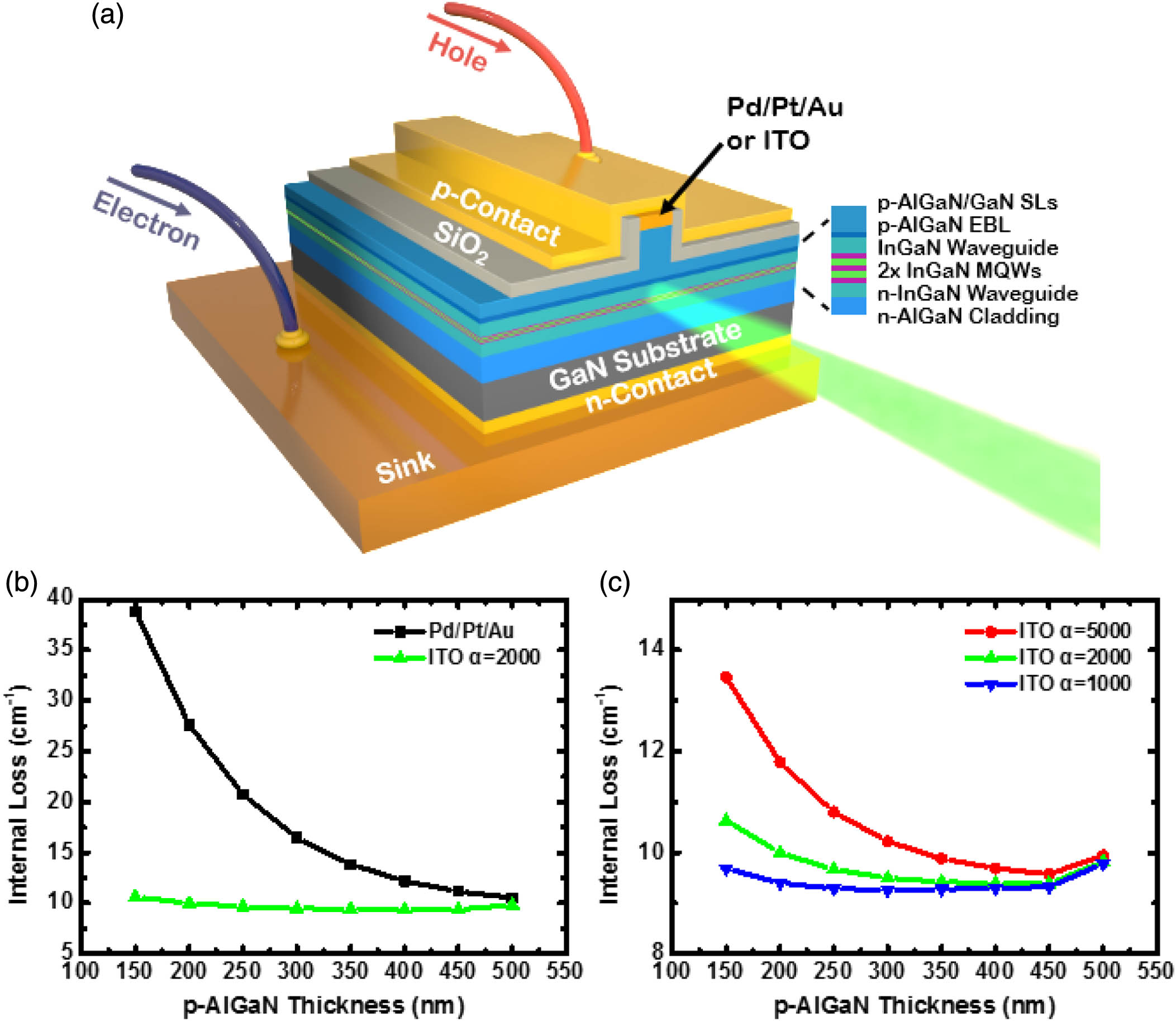
Absorption induced by activated magnesium (Mg) in a p-type layer contributes considerable optical internal loss in GaN-based laser diodes (LDs). An LD structure with a distributed polarization doping (DPD) p-cladding layer (CL) without intentional Mg doping was designed and fabricated. The influence of the anti-waveguide structure on optical confinement was studied by optical simulation. The threshold current density, slope efficiency of LDs with DPD p-CL, and Mg-doped CL, respectively, were compared. It was found that LDs with DPD p-CL showed lower threshold current density but reduced slope efficiency, which were caused by decreasing internal loss and hole injection, respectively.
polarization doping internal loss GaN laser diode Chinese Optics Letters
2021, 19(12): 121404
1 中国科学技术大学纳米技术与纳米仿生学院,合肥 230026
2 中国科学院苏州纳米技术与纳米仿生研究所,纳米器件与应用重点实验室,苏州 215123
氮化镓(GaN)基蓝光和绿光激光器在投影显示、激光加工、激光照明、存储等领域具有重要的应用前景与广泛的市场需求。本文着重介绍了GaN基蓝光和绿光边发射激光器的技术难点和相应的解决方案。在GaN基蓝光与绿光激光器中,就制备高质量InGaN/GaN多量子阱、减少内部光学损耗、增加空穴注入效率等方面分别介绍了一些结构与工艺方面的优化方法。简要介绍了垂直腔面发射激光器(VCSEL)、分布式反馈激光器(DFB)的研究现状。
半导体激光器 氮化镓 热退化 In偏析 内部光学损耗 载流子注入效率 semiconductor laser diode GaN thermal degradation In segregation internal optical loss carrier injection
1 中国科学技术大学纳米技术与纳米仿生学院, 安徽 合肥 230026
2 中国科学院苏州纳米技术与纳米仿生研究所纳米器件与应用重点实验室, 江苏 苏州 215123
高功率氮化镓基蓝光激光器在激光显示、激光照明和材料加工等领域具有很大的应用前景。通过优化蓝光激光器p-AlGaN限制层的生长温度,抑制了量子阱热退化,通过优化量子阱结构,改善了载流子分布,研制出了高功率蓝光激光器。利用变腔面反射率法获得蓝光激光器的内部光学损耗为6.8 cm -1,载流子注入效率为90%。在脉冲工作条件下,蓝光激光器的阈值电流密度为1 kA/cm 2,斜率效率为1.65 W/A,预计在6 kA/cm 2电流密度下,输出光功率能达到4 W;在连续工作条件下,激光器的阈值电流密度为1 kA/cm 2,由于封装散热性能不佳,斜率效率下降为1 W/A,预计在6 kA/cm 2的电流密度下,输出光功率为2.2 W。
激光器 氮化镓 蓝光激光器 热退化 内部光学损耗 载流子注入效率
Author Affiliations
Abstract
1 Key Laboratory of Nanodevices and Applications, Suzhou Institute of Nano-Tech and Nano-Bionics, Chinese Academy of Sciences (CAS), Suzhou 215123, China
2 School of Nano-Tech and Nano-Bionics, University of Science and Technology of China, Hefei 230026, China
Green laser diodes (LDs) still perform worst among the visible and near-infrared spectrum range, which is called the “green gap.” Poor performance of green LDs is mainly related to the p-type AlGaN cladding layer, which on one hand imposes large thermal budget on InGaN quantum wells (QWs) during epitaxial growth, and on the other hand has poor electrical property especially when low growth temperature has to be used. We demonstrate in this work that a hybrid LD structure with an indium tin oxide (ITO) p-cladding layer can achieve threshold current density as low as , which is only one third of that of the conventional LD structure. The improvement is attributed to two benefits that are enabled by the ITO cladding layer. One is the reduced thermal budget imposed on QWs by reducing p-AlGaN layer thickness, and the other is the increasing hole concentration since a low Al content p-AlGaN cladding layer can be used in hybrid LD structures. Moreover, the slope efficiency is increased by 25% and the operation voltage is reduced by 0.6 V for hybrid green LDs. As a result, a 400 mW high-power green LD has been obtained. These results indicate that a hybrid LD structure can pave the way toward high-performance green LDs.
Photonics Research
2020, 8(3): 03000279
Author Affiliations
Abstract
1 School of Nano Technology and Nano Bionics, University of Science and Technology of China, Hefei 230026, China
2 Suzhou Institute of Nano-Tech and Nano-Bionics, Chinese Academy of Science, Suzhou 215123, China
3 Key Laboratory of Nanodevices and Applications, Chinese of Academy of Science, Suzhou 215123, China
4 Vacuum Interconnected Nanotech Workstation (NANO-X), Suzhou Institute of Nano-Tech and Nano-Bionics, Chinese Academy of Sciences, Suzhou 215123, China
The inhomogeneous broadening parameter and the internal loss of green LDs are determined by experiments and theoretical fitting. It is found that the inhomogeneous broadening plays an important role on the threshold current density of green LDs. The green LD with large inhomogeneous broadening even cannot lase. Therefore, reducing inhomogeneous broadening is a key issue to improve the performance of green LDs.
Journal of Semiconductors
2019, 40(5): 052802


